
PCB Thermal Analysis for Engineers: A Practical Workflow

Updated: Aug 26

Run a steady-state power-map check first, add thermal vias and copper pours where junction temperatures exceed component ratings, then verify with a transient electrothermal simulation before you cut a prototype. That sequence catches the majority of thermal failures before they cost you a board spin.
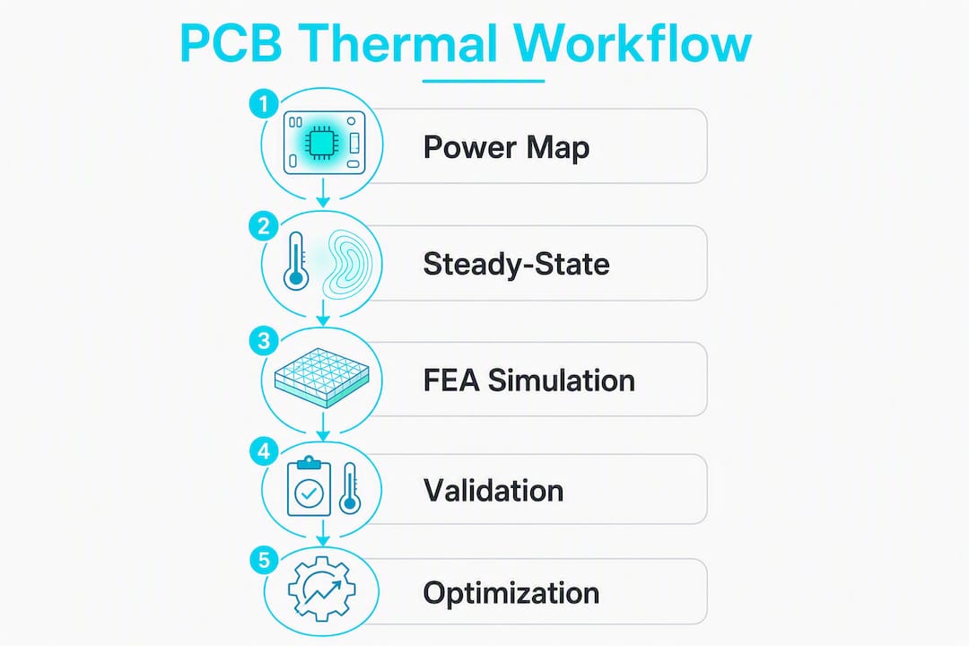
Generate a power map from your BOM and schematic: assign dissipation values to every active component and high-current trace.
Run a fast steady-state solver to locate hotspots. Anything above your derating threshold gets a layout intervention immediately.
Add thermal vias directly under hot pads, thicken copper pours on internal planes, and re-run before moving to transient analysis.
Pro Tip: Before reaching for a heat sink, ask whether you can reduce the heat source itself. A lower-RDS(on) FET or a higher-efficiency switching topology often cuts junction temperature more than any passive cooling addition.
Table of Contents
Why does PCB thermal analysis matter, and when should you run it?
What layout and hardware techniques actually reduce junction temperature?
How do you run a thermal simulation from power map to validation?
How do you interpret results and validate them against real hardware?
How does the Jewlztech Thermalysis Toolkit fit into a PCB thermal workflow?
The part of PCB thermal analysis most engineers underestimate
Why does PCB thermal analysis matter, and when should you run it?
Thermal failures are not random. They follow predictable patterns tied to power density, airflow, and stackup choices that are all set during design. Integrating thermal management throughout the design process rather than treating it as a post-layout check is the single biggest schedule saver available to a hardware team.
The consequences of skipping early checks compound quickly. Component derating violations shorten MTBF. Localized hotspots cause solder joint fatigue, especially under BGA packages where you cannot see the damage. High junction temperatures also shift transistor operating points in ways that degrade signal integrity and increase EMI emissions — a thermal problem that becomes an EMI problem is expensive to debug.
When to run which analysis:
Schematic and stackup stage: A lightweight lumped-parameter check using component datasheets and estimated copper areas. The goal is to flag any part whose power dissipation exceeds what the stackup can handle without intervention.
Placement and routing stage: A board-level steady-state simulation with actual component footprints, copper pour geometry, and via arrays. Early simulation reduces costly late-stage rework by surfacing layout-driven hotspots before traces are locked.
Pre-prototype sign-off: High-fidelity transient or electrothermal analysis, and CFD if the design lives in an enclosed enclosure with restricted airflow.
Triggers that demand an additional analysis pass: high-power ICs above 1 W, tight-pitch BGAs, power converters with switching losses, long high-current traces on outer layers, and any design going into an enclosed or sealed enclosure. The hardware engineer owns the early checks; a thermal or mechanical engineer should own CFD-level verification.
What layout and hardware techniques actually reduce junction temperature?
Layout changes are your highest-leverage tool. Changing PCB layout alone can reduce thermal resistance by up to 34%, and adding a soldered heat sink after achieving optimal layout yields an additional reduction of about 20%. Focus on layout first for the most cost-efficient thermal improvements. That ordering matters: optimize the layout first, then decide whether passive hardware is still needed.
Thermal vias
Place thermal vias in a tight array directly under the exposed pad of any power component. For multilayer boards, connecting heat sources to nearby interior copper planes via thermal vias reduces thermal resistance more effectively than enlarging distant copper areas. Filled or copper-plugged vias conduct better than unfilled ones, though they add assembly cost. A common starting point is a 3×3 or 4×4 array of 0.3 mm drilled vias on a 0.6 mm pitch under a QFN or DPAK pad.
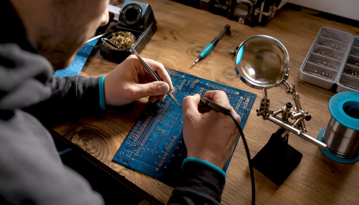
Watch for solder wicking into unfilled vias during reflow — it starves the thermal pad joint.
Stackup and copper planes
Layer count and copper weight directly control vertical conduction. A 4-layer board with 2 oz copper on the inner planes conducts heat to the board’s thermal mass far faster than a 2-layer board with 1 oz copper. Per JEDEC JESD51-based guidance, shorter vertical paths to copper planes reduce Rth more effectively in multilayer designs. Copper thickness on signal layers is a trade-off: heavier copper improves thermal spreading but complicates impedance control.
Passive hardware: heat sinks, TIM, and copper coins
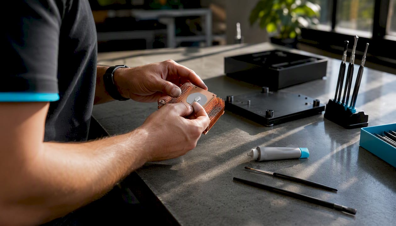
Heat sinks make sense when layout changes alone cannot meet the thermal budget. Always use a thermal interface material between the component case and the heat sink — even a thin layer of air gap increases contact resistance by an order of magnitude. Copper coins pressed into the PCB under high-power devices are common in RF and power electronics where the component footprint is small but dissipation is high. Metal-core PCBs are worth considering when the entire board runs hot, not just individual components.
Reducing heat at the source
Minimizing heat generated at the source through component selection and circuit efficiency is the single most effective thermal-management strategy. A synchronous rectifier replacing a Schottky diode, or a GaN FET replacing a silicon MOSFET, can cut dissipation by 30–50% before any layout change is made. Switching frequency trade-offs also apply: higher frequency reduces passive component size but increases switching losses in the FET.
Pro Tip: Optimize layout first to get the largest Rth reduction at zero BOM cost. Add active cooling only after layout and passive hardware options are exhausted. See the active vs. passive cooling decision guide for a structured framework.
How do you run a thermal simulation from power map to validation?
The workflow below is ordered. Skipping steps or running them out of sequence produces results that look plausible but mislead design decisions.
Build the power map. Assign a power dissipation value to every component and high-current trace. Pull switching losses from datasheet efficiency curves, not just quiescent current specs. Conduction losses on traces require actual RMS current and copper resistance at operating temperature.
Set boundary conditions. Define ambient temperature, airflow velocity and direction, board mounting orientation, and enclosure geometry. Simulated thermal resistance values are best treated as trend indicators because real-world chassis shape and airflow heavily influence absolute results. Garbage boundary conditions produce confident-looking garbage outputs.
Run steady-state analysis. Use a fast lumped or finite-difference solver. The goal is hotspot location, not precise temperature values. Flag any component whose predicted junction temperature exceeds 80% of its rated maximum.
Run transient or electrothermal analysis. Transient analysis reveals peak temperatures during load steps, startup surges, or fault conditions. Electrothermal coupling captures how resistance changes with temperature affect current distribution — critical for power converters and motor drivers.
Identify hotspots and iterate layout. Move components, add vias, thicken copper, adjust placement relative to airflow. Re-run steady-state after each significant change. Identifying hotspots early via thermal modeling is the first step before selecting any cooling method.
Validate with lab measurements. Thermocouples on board surfaces, IR camera imaging, and junction temperature estimation from VBE or RDS(on) shifts. Correlation within 10–15°C of simulation is a reasonable target for board-level steady-state.
Analysis type | When to use | Typical runtime | Deliverable |
Lumped steady-state | Schematic/stackup stage | Seconds to minutes | Hotspot flag, go/no-go |
Board-level FEA steady-state | Post-placement | Minutes to 1 hour | Temperature map, Rth per component |
Transient electrothermal | Pre-prototype | 1–4 hours | Zth curves, peak junction temps |
CFD (enclosure-level) | Sealed/complex airflow | Hours to overnight | Airflow map, system-level temps |
For meshing: refine the mesh near BGA thermal pads and exposed-pad packages. Coarser mesh on large copper planes is acceptable. Check solver convergence — residuals should drop at least three orders of magnitude before you trust the result. For heat transfer modeling approaches and the underlying math, the equations governing conduction, convection, and radiation each require different numerical treatment.
Workflow checklist:
[ ] Power map complete with switching and conduction losses
[ ] Boundary conditions documented (ambient, airflow, mounting)
[ ] Steady-state run complete, hotspots flagged
[ ] Layout changes applied and re-run confirmed
[ ] Transient analysis run for load-step and startup conditions
[ ] Lab validation scheduled with thermocouple and IR plan
Which thermal simulation tool should you use, and when?
Thermal analysis tools range from simple lumped models to computationally intensive simulations; the right choice depends on design stage and available compute time, not on which tool has the most features.
Approach by phase:
Early checks (schematic/stackup): A fast lumped-parameter or spreadsheet-based tool. Speed matters more than fidelity here. You need a go/no-go answer in minutes, not hours.
Mid-fidelity layout iteration: Board-level FEA or electrothermal solvers integrated with your PCB layout tool. The ability to import copper geometry and stackup directly from the layout file saves hours of manual setup.
High-fidelity verification: CFD-class tools for enclosure-level airflow, forced convection, and complex thermal coupling between boards in a chassis. Runtime is measured in hours; reserve this for pre-prototype sign-off.
Industry tools worth knowing:
Altium Designer includes thermal analysis features that pull copper geometry and component placement directly from the layout, making it practical for board-level steady-state checks during the routing phase. Altium’s resources on circuit board thermal analysis also cover passive technique integration.
Cadence Sigrity supports electrothermal co-simulation and is commonly used for package-level and board-level transient analysis where electrical and thermal domains are tightly coupled.
ST eDesignSuite PCB Thermal Simulator is a browser-based tool from STMicroelectronics designed for quick thermal checks on ST component-based designs. Useful for early-stage validation when the design is built around ST power devices.
Jewlztech Thermalysis Toolkit is a web-based, physics-focused engineering simulation toolkit covering conduction, convection, and radiation modes with a built-in material property database. It fits naturally into early and mid-fidelity thermal design checks and supports rapid engineering iteration without requiring engineers to build spreadsheet-based calculation models or use a high-compute workstation.
For engineers evaluating tools, the columns that matter most are model fidelity (lumped vs. FEA vs. CFD), simulation modes supported (steady-state, transient, electrothermal), PCB/CAD integration depth, licensing cost, and runtime per analysis. Evaluating simulation software alternatives across those dimensions gives a cleaner comparison than feature-count lists. Combining passive copper-based strategies with active forced-air cooling gives predictable results when both are designed together rather than one added after the other.
How do you interpret results and validate them against real hardware?
Treat every simulation output as a hypothesis, not a measurement. The number on the screen reflects your boundary conditions as much as it reflects the physics of your board.
Common pitfalls:
Wrong boundary conditions: Simulating in free air when the board lives in a sealed enclosure produces optimistic temperatures by 20–40°C in typical power electronics designs. Always model the actual thermal environment.
Inaccurate power inputs: Using datasheet typical values instead of worst-case dissipation at maximum load and maximum ambient. Thermal margin is eaten by exactly this assumption.
Ignoring mutual thermal coupling: Two adjacent power devices each running at rated dissipation will heat each other. Measured experiments show that copper fields and thermal vias significantly lower device thermal resistance, and that mutual thermal coupling becomes negligible under forced convection — but under natural convection, it can add several degrees to both devices.
Mesh errors: Under-meshing near BGA pads misses the steep temperature gradient at the die attach. Over-meshing large copper planes wastes compute time without improving accuracy.
Validation steps:
Place thermocouples on the PCB surface adjacent to the hottest component, not on the component case itself. Derive junction temperature using the package’s θJC and the measured case temperature.
Use an IR camera for a full-board temperature map. IR emissivity varies by surface finish — solder mask reads differently than bare copper. Calibrate with a known reference point.
For transient validation, log temperature versus time during a controlled load step and compare the shape of the Zth curve to simulation. A mismatch in the early time constants points to an error in the die-attach or package model; a mismatch at steady-state points to boundary condition errors.
Troubleshooting checklist:
Predicted hotspot not seen in lab? Check whether the physical board has more airflow than the simulation assumed, or whether the power input value was overstated.
Lab hotspot not predicted by simulation? Check for missing power sources (quiescent currents, gate drive losses), incorrect stackup copper weights, or missing via arrays in the model.
Simulation converges but temperatures seem too uniform? Check mesh density near high-power components — the solver may be averaging across too large a cell.
Pro Tip: Build a dedicated thermal test fixture that replicates the intended mounting orientation, enclosure geometry, and airflow path. A board tested flat on a bench in open air tells you almost nothing about how it will perform in a sealed enclosure with restricted convection.
How does the Jewlztech Thermalysis Toolkit fit into a PCB thermal workflow?
The Jewlztech Thermalysis Toolkit is a web-based engineering simulation platform for conduction, convection, radiation, steady-state, and transient thermal analysis. It provides engineers with physics-based thermal calculations, built-in material properties, and rapid design iteration without requiring engineers to build custom calculation models or purchase a dedicated high-cost simulation license.
Features engineers use in practice:
Built-in material and property database covering common PCB substrates, copper alloys, thermal interface materials, and enclosure materials
Steady-state and transient solvers with variable material properties across a wide temperature range
Support for multiple heat transfer modes in a single model (conduction through stackup, convection to ambient, radiation from board surface)
Web-based engineering workflow that enables rapid thermal analysis and design iteration without requiring engineers to build or maintain custom calculation models.
Where it sits in the workflow:
Use it at the schematic stage to run a fast steady-state check on your power map before layout begins.
Use it during placement to evaluate via array configurations and copper plane sizing against a thermal budget.
Use it as a pre-CFD evaluation step to confirm that layout-level changes have moved the design into an acceptable range before spending compute time on a full enclosure model.
A typical use case: an engineer working on a 48 V DC/DC converter identifies a predicted hotspot on the synchronous FET during a steady-state run. The toolkit flags that the current via array under the exposed pad is insufficient. Adding a second via row and increasing the inner copper plane area reduces the estimated Rth enough to bring the predicted junction temperature within the derating limit. That change takes 20 minutes to evaluate in the toolkit and would have required a full board respin to discover in hardware.
When the design involves complex 3D airflow, multiple boards in a chassis, or liquid cooling loops, escalate to a full CFD tool. The Thermalysis Toolkit is the right instrument for the early and mid-design stages where iteration speed matters most.
Key Takeaways
Effective PCB thermal analysis requires running the right analysis at the right design stage: power map and steady-state early, transient and CFD before prototype sign-off, and lab validation to close the loop.
Point | Details |
Run analysis early and often | Lightweight steady-state checks at schematic stage prevent expensive layout rework later. |
Layout changes first | PCB layout optimization alone can reduce thermal resistance by up to 34% before any hardware is added. |
Set accurate boundary conditions | Simulating in free air when the board lives in an enclosure can produce optimistic temperatures by 20–40°C. |
Validate with hardware | Use thermocouples and IR imaging to correlate simulation results; target within 10–15°C for board-level steady-state. |
Jewlztech Thermalysis Toolkit | Supports conduction, convection, and radiation analysis in a web-based engineering simulation workflow for early and mid-fidelity PCB thermal checks. |
The part of PCB thermal analysis most engineers underestimate
The standard advice is to run thermal simulation before prototyping. That is correct but incomplete. The deeper issue is that most engineers treat thermal analysis as a verification step rather than a design input. They finish the layout, run the simulation, find a hotspot, and then try to fix it within the constraints of a locked floorplan. That sequence is backwards.
The engineers who get thermal right use simulation to make placement decisions, not to check them. They know before routing whether a particular component needs to sit near a copper pour, whether a via array is needed under a pad, or whether the stackup needs an additional inner plane. That knowledge comes from running fast, low-fidelity checks early and often — not from a single high-fidelity run at the end.
The other underestimated factor is source reduction. A 10% improvement in converter efficiency at full load can eliminate the need for a heat sink entirely. That is a BOM cost saving, a reliability improvement, and a size reduction in one decision. Thermal simulation tells you where the heat goes; component selection determines how much heat you have to manage in the first place. Both levers matter, and the best thermal designs use both.
The Thermalysis Toolkit gives you fast, physics-based thermal checks without a heavy simulation license
Most PCB thermal analysis software is either too slow for early-stage iteration or too expensive for individual engineers and small teams. The Jewlztech Thermalysis Toolkit is built for the gap between a back-of-envelope calculation and a full CFD run.

The Thermalysis Toolkit provides conduction, convection, and radiation analysis in a web-based engineering simulation environment with a built-in material property database, transient and steady-state solvers, and support for variable material properties across a wide temperature range. Engineers can use it to evaluate thermal designs and compare design alternatives in minutes rather than hours. Its subscription-based access provides engineers with a practical thermal analysis platform without requiring a large capital software purchase.
If you are running thermal checks on a PCB design and want a faster path from power map to confident layout decisions, start a trial of the Thermalysis Toolkit at jewlztech.com.
Useful sources for deeper study
These references cover the technical foundations and tool-specific workflows behind the guidance in this article.
Circuit board thermal analysis (Altium) — Covers passive technique integration and early-stage thermal management; useful for understanding how thermal checks fit into the Altium Designer workflow.
PCB heat dissipation techniques (Altium) — Detailed overview of passive and active cooling combinations; good reference for mixed-strategy designs.
Thermal Analysis (Cadence resources) — Explains solver selection and the fidelity-versus-runtime trade-off; useful when choosing between lumped, FEA, and CFD approaches.
Influence of PCB layout on heat dissipation and mutual thermal couplings (MDPI) — Peer-reviewed experimental data on copper field and via effects on Rth; the most rigorous quantitative source in this list.
PCB Layout Thermal Design Guide (ROHM application note) — JEDEC JESD51-based guidance on stackup, via placement, and boundary condition selection; use this when setting up simulation inputs and interpreting Rth data.
Recommended
Comments